
Our Products & services
Click to view more details
Click on the product type to filter what you’re looking for.


Product and Service
Main Production
-
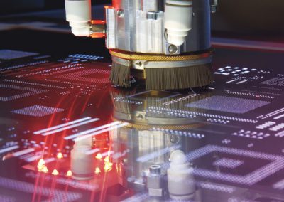
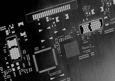
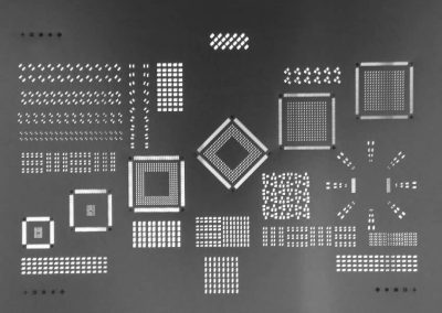
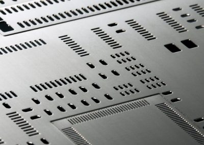
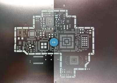
Laser Cut Stencil
Laser-cut is a subtractive process. The Gerber data is translated into a CNC-type language that the laser understands. The aperture is cut out by moving the laser head only, moving the table holding the stencil only or a combination of each. The laser beam enters inside the aperture boundary and traverses to the perimeter where it completely cuts the aperture out of the metal, one aperture at a time.
-
Electro Polished Stencil
During the PCB Stencil making process, the opening or aperture wall becomes rough due to the constant application of laser beams. This happens because the laser beam tends to melt the sheet material, which leads to some surface abnormalities called micro-burrs in the aperture wall. To solve this problem, Electropolishing is performed to smoothen the aperture wall. It promotes the easy transition of solder paste from the stencil to the intended PCB pads.
This process is performed through an acid rinse to control the aperture wall roughness by applying a specific voltage. Basically, it’s an inverted galvanizing process, where metal ions are dispensed in the acid bath. The SMT stencil is covered by an electrolyte solution so that the negative charge gets transferred to the solution by leaving positive charges on the stencil. Direct current is applied to the stencil, which removes the metal ions and compels them to move towards the negative pole.
Benefits of Electropolishing:
- Electropolished stencils offer high precision printing, especially for very small PCB pads.
- Uniform distribution of solder paste is possible due to the superb aperture wall finish
- It is easy to clean the electropolished stencils so that they can be used repeatedly.
- It increases the solder paste release rate by improving the surface finish.It improves corrosion resistance.
During this process, the entire surface, specifically the laser-cut aperture walls become smooth and free from the surface abnormalities.
Sometimes, Nickel plating is also performed to achieve the smooth opening/ aperture walls, but it has one limitation of reducing the overall dimension of aperture opening and requires artwork adjustment.
-
Nano Coated Stencil
The ongoing trend for miniaturization of electronic devices ensures that the surface mount assembly process will continue to provide new challenges. Components and stencil apertures are getting smaller and tighter in pitch. The demands on the solder paste printing process require improvements in technology.
Nano-coatings for stencils have been available for many years. The coatings are supplied in two common forms. The most common form is a multiple step liquid coating which is applied by wiping onto the stencil and drying in ambient air. A less common form of nano-coating is spray coated by stencil.
Benefit :
- Reduced bridging
- Reduced underside cleaning
- Improved solder paste release
- Improved yield
The cost to apply most nano-coatings is negligible when compared to the potential savings in cleaning materials, solder paste waste, yield improvements and avoidance of rework. If an increase in transfer efficiency is desired, then this can be achieved through the use of certain coatings.
-
Frameless Stencil
All our Stencils are available as frameless foils for mounting in Alpha Tetra and Vector Guard foil frames.
ALPHA TETRABOND is the culmination of “frameless” stencil development; an elegantly simple system designed to enhance the rigidity of the foil, making safe mounting and demounting an easier proposition. Innovatively encompassed in a thin, one piece aluminum extrusion, ALPHA TETRABOND stencil foils are designed for use with Tetra and VectorGuard foil tensioning frames and are backward compatible with the majority of frames currently in the market.
Alpha TetraBond Features and Benefits :
- Excellent rigidity for durability and ease of use
- Safe to use, no sharp edges
- Image float is eliminated
- Minimal storage space requirements
- Saves transport costs
-
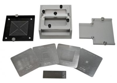
Custom-Made Mini Stencil, Template and Metal Squeegee Blade
We manufacture mini stencil, template and metal squeegee from stainless steel alloys with optimum material properties that guarantee you the best possible printing performance. We also support customer-specific design as their required. Custom-made is possible for corresponding to your usage.
Mini stencils are laser cut stencils custom-made for your own printed circuit boards using your part drawings from the part data sheet, Gerber or CAD files. Small stencils that are used mainly for BGA re-work. It is designed to deposit precise amounts of solder paste for single BGA footprints on loaded PCBs. These precision stencils mimic the footprint and aperture sizes used in the original production stencil.
Template is a customized form, mold, or pattern used as a guide to making something. This is available based on specific design with material stainless steel alloys and maximum thickness 23mil.
Metal Squeegee is a tool with a flat, smooth blade, used to remove or control the flow of liquid on a flat surface. It is used for cleaning and improve a positional accuracy in printing and a stability of solder.
-
Modification and Stencil Retention
We provide modification and retention service for new or used stencils. For more detail, please contact our sales administration
-
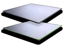
SMT/WAVE/REFLOW PALLET
SMT Pallet will reduce rework of boards, and increase the ease of manufacture. SMT tooling, fixture, SMT Pallet, or Reflow Pallet, which is a special design fixture or tooling, can be used for solder paste printing, pick and place and reflow soldering and the available thickness is always 3-4mm.
Wave solder pallet is the most reliable and inexpensive method of soldering through-hole components on circuit boards. They are designed to meet unique requirements to solve complex processes.
- Wave solder pallets mask SMT components (ground planes, gold fingers and mounting holes) while exposing the circuit board to the wave only where solder is required.
- They provide thermal protection for printed circuit board areas that are heat sensitive.
- A wave solder fixture provides support for the PCB throughout the wave solder process.
SMT/Wave solder pallets are made of composite materials with advantageous features such as:
- High temperature compatibility to endure repeated cycles through the re-flow.
- Dimensional stability to ensure board alignment is consistent.
- Very low moisture absorption.
- Low heat absorption.
- Chemical resistance for increased durability through the harsh cleaning process
Please provide your gerber or CAD data to our engineer team or any special requirement in design or material. We can design based on your requirement.
-
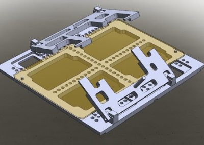
JIG & FIXTURE
Jigs and fixtures are production tools used to accurately manufacture duplicate and interchangeable parts. Jigs and fixtures are specially designed so that large numbers of components can be machined or assembled. Special design available by providing drawing in gerber or cad data by customer.
All custom-made size and model are available, please contact our sales administration.
High Quality Stencil
-
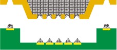
Step Stencil
Numerous SMD applications require a large number of very different components on a circuit board and therefore different quantities of solder paste have to be applied in one printing pass. These differences in solder paste requirements can no longer be leveled out by the pad geometry and size of the apertures alone; what they need are stencils which have partial or local steps in thickness. They are called step, step-up/step down or multi-level stencils
- Step-Down Stencil :
Reducing the thickness of certain area in stencil to lessen the Tin volume of specified components in soldering process, and no affection of stencil cleaning. This step-down stencil will be helpful to solve printing defect for special bump (such as with label) of PCB.
- Step-Up Stencil :
Increasing the thickness of certain area in stencil to add Tin volume for designed components in population process, and it is especially suitable for through hole reflow solder artwork (such as plug-in, Dip components reflow solder).
- Multi-Level step stencil :
Reducing and increasing the thickness of stencil for certain area, on the same stencil. It means there are three different thicknesses in the same stencil, to meet different requirements of Tin volume.
-
Electroform Stencil (E-Form)
Electroform technology delivers ultimate control over stencil thickness and uniformity, ensuring outstanding paste volume consistency for fine pitch applications. Electroform stencils provide superior performance and ensure seal contact to the pad, pad paste deposit and a greater percentage volume of paste on pad. Electroform stencils are very effective for printing paste on SMT boards with fine pitch parts spread over a large area and provide excellent print performance for applications with miniature BGAs, ultrafine pitch QFPs and small components such as 0201.
Benefits:
- Smooth, trapezoidal sidewalls maximize solder paste release
- High Seal Technology for 1:1 stencil open to pad, for PB-free applications
- Improved solder paste release ideal for Pb-free paste formulation.
-
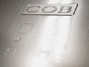
COB Stencil (Embossed)
COB (Chip On Board) stencil is used for printing on the PCB with pre-mounted devices (such as bare chip ) or PCB with some convex parts on its surface. This stencil is produced by electro-forming method. This stencil is developed in order to correspond to PCB which some components were mounted on PCB. It is possible for COB stencil to mount additional components on ready mounted PCB.
Features :
- Applicable for conventional SMT line!
- Enable to be shorten line numbers and to reduce production cost!
- Excellent durability on long term usage!
-
3D & PH STENCIL
3D stencil is the stencil to mount IC packages and passive components on a cavity PCB in order to decrease the mounting both space and height enabling both miniaturization and a high function on circuit.
PH stencil has been developed for super high density printing is special stencil that is corresponding to 0.3mm pitch components, 0603mm components such as Flip chip. PH stencil has two layers, which one is metal layer and the other one is plastic layer. It provides high dimensional precision, high contactness between a pcb and a stencil, and excellent passing-throgh of solder paste.
-
Nickel Stencil
Nickel stencil is another material that can be used for SMT Stencil. This material is suitable to use in precision etching or eletroforming process as well. For more information, you need to contact our sales administration.
-
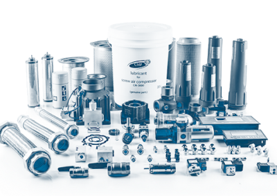
Other Supporting Parts
Consummables:
- Plastic Squeegee Blade
- Rubber Squeegee Blade
- Cutting blades
- Stencil cleaning wipes
- Stencil cleaning rolls
- Stencil cleaning liquid chemical
- Glue/Adhesive
- Chemical
- Labeling
- Packaging
Machine & Tools:
- Hand-held stencil cleaning kit
- Ultrasonic machine
- Pneumatic stencil cleaning machine
- PCB separator machine
- Wire cutting & Stripping machine
- Dispensing system
- Laser printing machine
- Soldering device
- Compenent lead former & cutter
- Robotic soldering machine
- Thermal profiler
- Other machinery spare parts
- Digital multimeter
- Cutting tools