MAIN PRODUCTION
Electro Polished Stencil
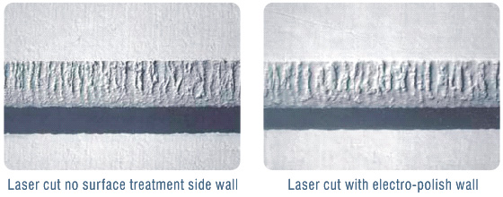
During the PCB Stencil making process, the opening or aperture wall becomes rough due to the constant application of laser beams. This happens because the laser beam tends to melt the sheet material, which leads to some surface abnormalities called micro-burrs in the aperture wall. To solve this problem, Electropolishing is performed to smoothen the aperture wall. It promotes the easy transition of solder paste from the stencil to the intended PCB pads.
Benefits of Electropolishing:
- Electropolished stencils offer high precision printing, especially for very small PCB pads.
- Uniform distribution of solder paste is possible due to the superb aperture wall finish
- It is easy to clean the electropolished stencils so that they can be used repeatedly.
- It increases the solder paste release rate by improving the surface finish.It improves corrosion resistance.


More Info
Electropolishing is performed through an acid rinse to control the aperture wall roughness by applying a specific voltage. Basically, it’s an inverted galvanizing process, where metal ions are dispensed in the acid bath. The SMT stencil is covered by an electrolyte solution so that the negative charge gets transferred to the solution by leaving positive charges on the stencil. Direct current is applied to the stencil, which removes the metal ions and compels them to move towards the negative pole.
